

|
 |


|

|
|
|
|
| ■ 2.5D, 3D Package |
■ CIS / LED |
| ■ TSV |
■ IGBT |
| ■ Interposer |
■ MEMS |
| ■ WL-CSP/FO-WLP |
■ Bumping |
|
| |
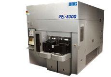
■ Variable Lens NA and 1:1 Dyson type Optical System
■ Large Exposure Field : 52x33mm2
■ User Friendly Reticle Design (max.8 fields)
■ Outgas Protection Unit for Optics
■ Handling System for thin Wafer, TAIKO Wafer and warped wafer
|
| |
| ■ Exposure Wavelength |
ghi-line, gh-line, i-line |
| ■ Resolution |
2 μm L/S (for 2 μm thickness photoresist) |
| ■ Depth of Focus |
≧10μm |
| ■ Initial Intensity |
≧2700mW/cm2 |
| ■ Exposure Uniformity |
≦ 3% (ghi-lines) |
| ■ Exposure Field |
52 x 33 mm2 |
| ■ Overlay Accuracy (machine-to-self overlay) |
≦ 0.5μm (|AVE|+3σ) |
| ■ Wafer Size |
6, 8, 12” |
| ■ Dimension / Weight |
3460(D) X 2260(W) X
2500(H) / 5500Kg |
|
| |
■ Backside Alignment
■ Exposure/Non-Exposure Function for Wafer Edge
|
|